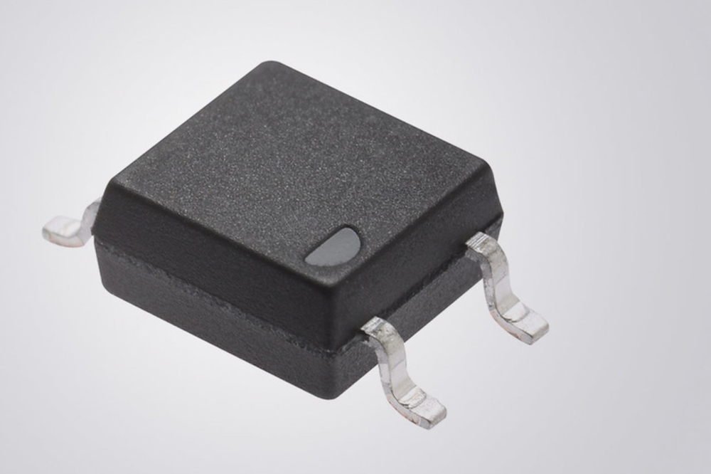
Boosting performance with the merged p-i-n SiC Schottky diode

Delivering greater reliability at high efficiency, the merged p-i-n SiC
Schottky diode combines a low forward voltage with high surge-current
capability.
BY LLEW VAUGHAN-EDMUNDS FROM NAVITAS SEMICONDUCTOR
The wide bandgap revolution in power conversion is well under way. To fulfil efficiency and power density targets in energy-conscious applications, designers are now rejecting silicon devices in favour of alternatives delivering superior performance.
Offering the greatest commercially maturity within the wide bandgap fraternity is SiC. Producers of this class of semiconductor have now released several generations of diodes and power MOSFETs, each offering successively improved performance. Sales of these devices have soared in recent times to hit nearly $3 billion last year, and growth is forecast to continue at around 40 percent per year as deployment expands into evermore applications.
SiC devices outperform their silicon counterparts in both conduction and switching characteristics. First to market within this family of power devices is the SiC Schottky barrier diode. Compared with the silicon fast-recovery diode, it has a lower forward voltage and a superior reverse recovery. One upshot of these strengths is a tremendous reduction in overall energy losses. Yet another merit of the SiC Schottky barrier diode is a stable reverse-recovery time over the full operating temperature range. In comparison, the silicon fast-recovery diode is impaired by an lengthening recovery time at higher temperatures.
Figure 1. MPS diodes combine p-i-n and Schottky diode attributes.
However, the SiC Schottky barrier diode is far from perfect. All Schottky diodes, regardless of material system, are inherently vulnerable to current surges. This is a known hazard in power-factor correction circuits, used in power supplies for converters and inverter systems.
One option for addressing this issue is to turn to p-i-n diodes, which offer greater reliability in such situations. However, reliability is traded for reduced efficiency, due to a higher forward voltage. It’s not a great compromise, as a lower energy efficiency is undesirable. In equipment such as server power supplies, a diminished efficiency leads to a higher electricity bill, increased cooling management and a slower return on investment.
A compelling solution is the merged p-i-n SiC Schottky (MPS) diode. This device marries the best features of Schottky and p-i-n diodes in a single device by combining the surge-current robustness and low reverse leakage of the p-i-n diode with the low forward voltage of the Schottky structure. Equipped with a superior breakdown voltage, excellent reverse-recovery characteristics, stability over temperature, and the high-temperature operating capability associated with all SiC devices, the MPS diodes that have been introduced in power factor correction and boost circuits are enhancing reliability and significantly increasing the overall efficiency of the power-conversion system.
Figure 2. Low-current, forward current-voltage (I-V) characteristics for 10 A SiC MPS diode.
Design and optimisation
A key difference between a conventional Schottky part of the device structure and the MPS diode is that the latter contains additional p-doped wells, implanted in the drift zone. These wells form a p-ohmic contact with the metal at the Schottky anode, while also creating a p-n junction with the SiC drift layer. The result is effectively the combination of a Schottky diode and a p-i-n diode, connected in parallel (see Figure 1).
With this design, in normal operation the Schottky carries almost the entire current. On the other hand, during high-current surges, the voltage across the MPS device rises, causing conduction in the drift layer of the p-i-n diode. As this intrinsic diode has a lower resistance than the Schottky, current is diverted, reducing dissipation and relieving thermal stress.
When the MPS diode operates under reverse bias, the maximum field strength occurs across its drift region. This contrasts with the situation in a standard Schottky architecture, where the greatest field strength occurs at the metal barrier. A downside of the Schottky diode is that imperfections in the barrier allow a relatively large leakage current to flow. That’s not the case with the MPS diode, which benefits from moving the maximum field strength away from the metal barrier. This design ensures that the leakage is lower than that of a standard SiC Schottky diode.
By optimising the dimensions and doping of the p-type wells, device designers can engineer the forward voltage drop, surge-current capability and leakage current of the MPS diode to meet specific requirements. Additional improvement comes from thinning the substrate below the drift region. This trims the MPS forward voltage and the thermal resistance between the Schottky area and back-side metallisation, leading to lower energy losses, enhanced thermal efficiency and greater reliability.
At Navitas, we have an enviable track record in developing and producing SiC MPS diodes. Now in their fifth generation, our 650 V SiC MPS diodes feature a high surge-current capability and a low forward voltage to minimise losses in the forward-biased mode. Our devices also offer an extremely low reverse-leakage current and high avalanche robustness. It is a combination of attributes that comes from optimising the device architecture and engineering the barrier metallurgy to ensure an ultra-low Schottky barrier height of just 0.88 eV at 25 °C.
One of the downsides of typical Schottky and MPS diodes, which feature a titanium metal barrier, is a trade-off between the Schottky barrier height and the reverse leakage current. Thanks to our novel, proprietary barrier metal, our MPS SiC diodes have a Schottky barrier height that’s more than 26 percent lower than alternative titanium-barrier devices, and a leakage current of just 100 nA – that is at least six times lower than the norm. In addition, our devices offer enhanced shielding of the Schottky metal interface, minimising any increase in reverse leakage current at higher voltages.
We have measured the forward current-voltage characteristics of these diodes at low currents and at temperatures from 25 °C to 175 °C (see Figure 2). These results reveal consistent linearity across this wide temperature range, indicating a stable Schottky barrier height, indicative of a good spatial homogeneity of the Schottky metal interface.
There is a small increase in the Schottky barrier height. That’s a common tendency amongst MPS diodes from various vendors. One way to evaluate this increase is to consider ‘ideality’, a measure of how closely the diode’s behaviour conforms to the ideal diode equation under different conditions. Ideality typically decreases with temperature, and has a value that’s close to 1 in well-behaved diodes under normal conditions. If there are deviations from this value, they tend to come from unwanted effects, such as recombination currents and parasitic series resistances. Note that real-world diodes can depart from ideal behaviour, and often display an ideality greater than 1.
We have also recorded the current-voltage characteristics of our MPS diodes at higher currents (see Figure 3). These plots, taken at various temperatures, show that there is a cross-over from unipolar (SiC Schottky) to bipolar (p-i-n) operation at about 90 A at 25 °C. This cross-over decreases to 50 A at 150 °C. Our plots also show a lowering of the knee-voltage at higher temperatures, which helps maintain a low temperature co-efficient of the on-state voltage drop at the rated current of 10 A.
To benchmark our devices, we have compared the capacitance-voltage curves of our diodes with those of rival products. These plots reveal that our MPS diode has one of the lowest values of capacitance charge, which ensures low reverse-recovery losses.
The low capacitance charge also enables our MPS diodes to have a good value for the common figure-of-merit for this device, defined as the product of capacitance charge and forward voltage. While improvement on one of these fronts tends to be detrimental to the other, a good figure of merit balances a low forward-voltage drop, key to trimming power losses, with a low capacitance charge that ensures superior switching performance. Attaining the lowest possible value for each helps to enhance the overall diode performance in power electronics applications.
Another important characteristic for the MPS diode is its level of avalanche robustness. We assess this with unclamped inductive switching tests. Values for the current waveform under unclamped inductive switching and current-surge conditions reveal a high value for the non-repetitive surge current, confirming our diode’s robustness (see Figure 5).
Figure 6. Navitas MPS diodes in a desaturation detection circuit and an interleaved power-factor correction (PFC) circuit.
Made for TV
Our MPS diodes can make a positive contribution to a number of applications. They offer a superior performance in: boost circuits, which raise the solar-panel output voltage to the 450-600 V required for the inverter; and in power-factor correction circuits, which are mandatory in line-powered applications above 75 W, according to IEC/EN 61000-3-2. Power-factor correction circuits are used in power supplies for telecom equipment, for data centre servers and for lighting systems.
SiC MPS diodes can also deliver benefits in consumer devices, such as televisions. With the advent of 4K UHD, the latest displays are demanding significantly more power than their predecessors, leading to a greater emphasis on efficiency, for both realising a suitable energy rating and for maintaining proper performance. As well as satisfying this requirement, efficient power supplies usually improve the performance of the display. Often the power supply is positioned directly behind the display, and if it generates too much heat due to a low efficiency, this impairs colour rendition.
We offer our SiC MPS diodes in various package options, which can deliver several advantages in different applications. For high-voltage sensing circuits, like desaturation detectors for overcurrent protection, as well as in the gate-drive bootstrap circuits of high-side switches (see Figure 6), the DO-214 and TO-252-2 packages are ideal solutions.
On the other hand, the TO-247-3 package provides extra flexibility when high-power density is required, and can help reduce the bill of materials in applications like interleaved PFC circuits, which share a common cathode between two diodes.
The key point is that SiC MPS diodes are compelling direct replacements for Schottky diodes in circuits that need to combine a high energy efficiency with robustness and reliability when exposed to surge currents. Such conditions occur when powering highly capacitive or inductive loads, or when the power quality of the main AC line is poor. As a straightforward drop-in replacement, our devices are easy to design-in for a significant boost in power-conversion efficiency.


